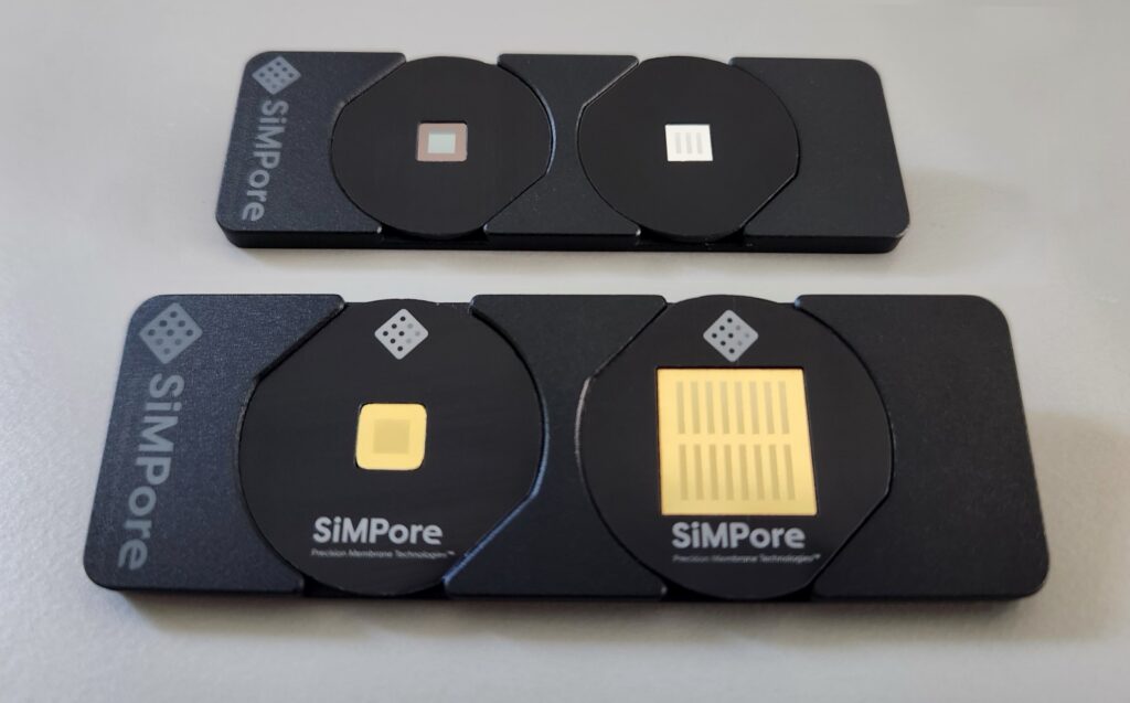
Custom Capabilities
Using custom fabrication to meet your needs, we fulfill custom silicon membrane fabrication requests for a wide range of applications.
Popular Custom Solutions
We offer services ranging from genomic and photonic biosensors and microfluidic cell culture to protein and nanoparticle separations and high resolution, environmental electron, x-ray microscopy, and silicon membrane fabrication. Below are some of our most popular custom solutions including custom silicon membranes.

Silicon Wafer Specifications
- 100 and 150 mm diameter preferred
- Range of thickness, orientation, resistivity, type, etc.
- Alternative Materials: Possible

In-House Mask Design & Lithography
Specifications
- Feature size resolution to 350 nanometers (line/space resolution)
- Capabilities: Hard/Soft Contact & 5x reduction stepper technology
- Layer-to-layer Alignment: 0.05 µm to 5 µm (Substrate dependent)
- Front-to-back Alignment: <5 µm to 20 µm (Substrate dependent)
Silicon-Based Deposition
- Amorphous Silicon: PVD deposited 5 to 50 nm thick
- Single/Poly Crystalline Silicon: As thin as 25nm thick
- Silicon Dioxide: Thermal, Sputter, or PECVD 10-4,000 nm thick
- Silicon Nitride: Stoichiometric and Si-rich LPCVD 5-2,000 nm thick

Metal-Based Deposition
- e-Beam and/or thermal evaporation of Al, Au, Ag, Cr, Ti, Ge, Ni, and more at ~3-200 nm thick
- Lift-off Features: Down to 5 µm

Surface Functionalization
- Wide range of monolayer-forming chemistries
- Chemical Vapor Deposition or Anhydrous Solvent / Solution deposition processing

Device Packaging
- Singulation by multiple methods – Customizable side profile
- Pick-and-place packaging of dies into trays
- Robotic assembly into devices
- Laser marking of wafers and individual dies or devices
Laser Processing
- Debris-free, non-contact die singulation
- Ultra-Fast / Ultra-Short Pulsed laser marking, <12 micron spot size
- Multiple laser processing / converting systems: CO2, MOPA, pulsed ns/ps/fs
Popular Membrane Materials
While we will custom-create any substrate for your needs, we most often find ourselves working with these popular custom silicon membrane fabrication materials.
Pure Silicon
- Amorphous, Single Crystal, or Nanocrystalline
- Sputter deposited 5 to 50 nm thick
- Nanocrystalline films are nanoporous with tunable pore sizes from 5 to 75 mm
Silicon Dioxide
- Amorphous silicon dioxide
- G-FLAT™ exclusive ultra-flat oxide
- Thermal, Sputter, or PECVD deposition
- Thicknesses from 20 to 4000 nm
Silicon Nitride
- Amorphous silicon nitride
- LPCVD Low stress – tunable
- Thicknesses from 5 to 2000 nm
- Ultra-flat suspended membranes
Send us a brief summary of your project’s requirements and we’ll get back to you with a custom evaluation.
Please note: This form is for custom product requests only. Please use the cart to generate a quote for standard inventory.
"*" indicates required fields